Tuesday, February 7, 2023

Bootstrapped collector loads

This post is a part of the series on audio amplifier feedback. The contents of the series can be found here.

A bootstrapped collector load is a pair of resistors connected in series, with their common point actively driven, often by a unity gain buffer via a large capacitor:

Bootstrapped loads have been popular in audio amplifiers for more than 50 years, although these days they are largely replaced by constant current sources.

The work of a bootstrapped load is easily understood. Because of the unity gain buffer, the right side of the capacitor $C$ (see the schematic above) sees the same potential as the bottom end of $R_2$. As long as the voltage across the capacitor is relatively stable, the voltage across $R_2$ is relatively stable, and so is the transistor's collector current flowing through $R_2$. In particular, the collector current changes only a little with changes in the collector potential (e.g. an audio signal), as if the collector load resistance is large.

Quantitatively, it is obvious that at DC, $R_1+R_2$ is the only load that sets the quiescent collector voltage. To find out AC response, one needs to e.g. write down node equations, which reveal that a bootstrapped load presents a frequency dependent impedance of the form $$Z = (R_1 + R_2) \times (1+s T_z)$$

where $T_z = (R_1 || R_2) C$.

The impedance increases with frequency at 20dB/decade, as would the impedance of an inductor. Effectively, a bootstrapped load is a synthesized inductor with the series resistance $R_1+R_2$ and the inductance $L = R_1 R_2 C$. For example, with R1=R2=1kOhm and C=10uF, the equivalent inductance L=10H.

In a real circuit, this synthesized inductor is not the only collector load - connected in parallel to it are the output impedance of the transistor and the input impedance of the buffer. If this input and output impedances are lumped into Ri:

then the combined collector load has the form $$Z = {R_i || (R_1 + R_2)} \times {{(1+s T_z)} \over {(1+s T_p)}}$$ where $T_z = (R_1 || R_2) C$ as above and $T_p = {{ (R_1 + R_2) \over (R_i +R_1 + R_2) } C}$.

I will look more into the behavior and practical uses of a bootstrapped load in separate posts.

Friday, January 20, 2023

High Precision Composite Op-Amps, Part 5 - Cart Before Horse


This post is a part of the series on audio amplifier feedback. The contents of the series can be found here.

In my previous post on this topic, I gave a couple of practical examples of composite amplifiers with the topology described by John D. Yewen's article in Electronics & Wireless World, February 1987 and promised we can do even better.

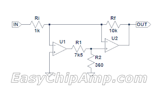
One of the issues with Yewen's topology:

is that R1 R2 (in the schematic above) attenuate the signal amplified by U1, which causes U1 to work extra hard, or, more precisely, work with a higher input signal. As was discussed previously on this blog, this affects the linearity of U1's input stage and adds distortion that cannot be corrected by feedback.

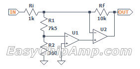
One way to address this issue is to use a better opamp as U1, but it is much easier to move the divider to U1's input:

R1 R2 should be large compared to Ri to avoid an unwanted noise gain increase and a loop gain reduction (see the discussion in my previous post), but otherwise this works exactly the same as Yewen's composite, only with lower distortion.

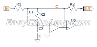
Naturally, this approach also works with frequency dependent dividers:

Friday, January 13, 2023

High Precision Composite Op-Amps, Part 4 - A Practical Composite Chipamp with LM1875

This post is a part of the series on audio amplifier feedback. The contents of the series can be found here.

In my previous post on this topic, I discussed the role of the voltage divider in John D. Yewen's composite op-amps (see his article in Electronics & Wireless World, February 1987) and improving the composite's loop gain at audio frequencies by making the divider frequency dependent.

Towards the end of the previous post, I promised that this approach works in hardware, too, so here are two practical examples.

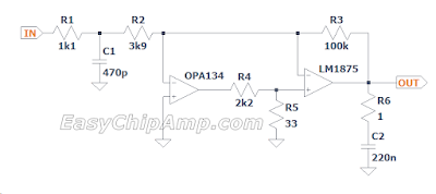
The first is a plain Yewen composite with two dissimilar opamps - an OPA134 and an LM1875:


The divider (R4R5) attenuates the output of the OPA134 by 33/(2200+33)≅-36dB, which together with the opamp's GBW of 8MHz places the zero (see my previous post for an explanation) at about 130kHz. It is kind of low, but in testing, placing the zero at a higher frequency made for poor clipping performance. With such a divider, the OPA134 adds about 16dB of loop gain at 20kHz (more at lower frequencies), and this composite produces 0.003% THD at 1kHz, 20W into 8ohm, or about 1/6 of the distortion of a standalone LM1875.

The second example is a composite with the same opamps and a frequency dependent voltage divider C4C5R10:


The improved divider adds a pole at 2kHz and a zero at 150kHz, increasing the loop gain by another 16dB at 20kHz while maintaining stability and clipping similar to that of the first composite. With a careful PCB layout, this composite should be able to deliver 0.001% of THD at 1kHz, 20W into 8ohm.

Note that for both versions, the Zobel network (R6C2 and R11C6, respectively) with the values shown is required for stability.

Can we make the composite still better? Yes we can! Stay tuned...