Saturday, February 3, 2024

Current Dumping: Fine Print

This post is a part of the series on audio amplifier feedback. The contents of the series can be found here.

In the previous post, I explained how current dumping works on an intuitive, qualitative level. Let's go into the next level of detail.

A current dumping amplifier is a feedback amplifier consisting of a low distortion, low power amplifier A and a high-power, distorting buffer ("current dumper", here Tr1 and Tr2)  inside a common negative feedback loop:

Negative feedback reduces, but not completely eliminates, the distortion that the current dumper adds to the signal. From my earlier post, the share of that distortion that remains at the output (point D at the schematic above) after the negative feedback is applied is given by the Error Transfer Function $${ETF={1 \over {1- A \times B}}}$$ where $A$ is the transfer function (basically, the frequency-dependent gain) of the integrator composed of A,R1,C1, and $B$ is the transfer function of the feedback network. In this case, the feedback network has unity gain and is connected to the inverting input of the integrator, so $B=-1$, and $${ETF={1 \over {1+ A}}}$$ Therefore of the total open loop distortion $\epsilon$ of the current dumper, at point D we observe $$\epsilon _D={\epsilon \times ETF}=\epsilon {1 \over {1+ A}}$$ Since the current dumper adds distortion $\epsilon$, for this to happen, the input of the current dumper (point A at the schematic above) should see "pre-distortion" $$ \epsilon _A = {\epsilon_D - \epsilon}={{\epsilon {1\over {1+ A}}}-\epsilon}=-\epsilon{A \over {1+ A}}$$ At the load, $\epsilon_A$ and $\epsilon_D$ combine in reverse proportion to the impedances of R2 and L1: $$\epsilon_{LOAD}\propto {\epsilon_A Z_{L_1} + \epsilon_D Z_{R_2}}$$ Note that the load impedance affects the absolute level of the combined signal at the load but not the proportion of $\epsilon_A$ to $\epsilon_D$.

Combining the last three equations and dropping the common denominator $1+A$: $$\epsilon_{LOAD}\propto {\epsilon (Z_{R_2} - A  Z_{L_1})}$$

Clearly, the perfect cancellation of the current dumper's distortion occurs when $$Z_{R_2} = A  Z_{L_1}$$

For the implementation above, under ideal conditions, $Z_{R_2}= {R_2}$, $Z_{L_1}= s {L_1}$, $A=1/{(s R_1 C_1)}$, and the perfect cancellation means

$$R_2={L_1 \over {R_1 C_1}}$$

which is the result from [1]: "For the linearity of Tr1 and Tr2 to be immaterial then L must equal RRC".

However, by going through the algebra above, we obtained a more general and quite remarkable result: a perfect distortion cancellation requires the ratio of $Z_{R_2} /  Z_{L_1}$ to mimic the amplifier's loop gain $A$. This gives us the freedom to make current dumping work under less than ideal conditions and in different implementations than above. Stay tuned.

References

  1. P. J. Walker and M. P. Albinson, "Current Dumping Audio Amplifier," presented at the 50th AES convention, March 1975.
  2. S. Takahashi and S. Tanaka, “Design and Construction of a Feedforward Error Correction Amplifier,” JAES vol. 29, pp. 31-37, Jan/Feb 1981.

Monday, January 29, 2024

Current Dumping Revisited

This post is a part of the series on audio amplifier feedback. The contents of the series can be found here.

Current dumping is a way of constructing a power amplifier where a low-power, low-distortion amplifier is used to correct the distortion of a higher-power, but less linear, amplifier ("current dumper"). The underlying assumption is that it is easier to construct a low power, low distortion amplifier than a high power, low distortion amplifier.

Current dumping was introduced by quintessential English audio company Quad and was used in a series of Quad's power amplifiers starting with the Quad 405. Quad's founder, P. J. Walker, presented the concept at the 50th AES convention in 1975 [1].

There has been much interest and public discussion of current dumping in late 1970s and early 1980s. While most reviewers used more or less complicated math to explain why and how current dumping works, the basic implementation is easy to understand on an intuitive level.

The following schematic is from Walker's original AES paper:

Here, A is the low power, low distortion amplifier, and Tr1 and Tr2 form the "current dumper". The load is connected to both A (via R2) and the current dumper (via L1).

The feedback for A is taken from the output of the current dumper. It is easy to see that for the feedback signal, A, R1 and C1 form an inverting integrator. As usual, the integrator adds a phase shift of 90° (on top of inverting) and amplification, with gain falling by 20dB/decade as frequency increases, reaching unity at

F0 = 1/(2π×R1×C1) 

With the values shown in the schematic above, F0 4.82MHz. The gain of this integrator at any other frequency is

G = F0 / Fx

For example, at 20kHz the gain is 4,820 / 20 = 241, or 47.6 dB with the values shown. As in any other negative feedback amplifier, the integrator's gain works to reduce the open-loop distortion of the current dumper by a factor of  (1+G).

The residual distortion from the output of the current dumper is fed to to the load via L1, which adds 90° of phase lag. Since L1's impedance increases with frequency, the distortion level at the load falls with frequency at 20dB/decade. The same residual distortion is amplified by the integrator and appears at its output (and, via R2, at the load). Here, the level also falls with frequency at 20dB/decade, but the phase shift is 270° (180° to account for inverting and 90° for integrating), that is, the phase is opposite to the distortion coming via L1. Since the levels are proportional and phases are opposite, with the right choice of R2, the residual distortion from the current dumper can be cancelled.

According to Walker, perfect cancellation occurs when L1=R1×R2×C1. In the language of the AES paper, "For the linearity of Trl and Tr2 to be immaterial then L must equal RRC". This conclusion, however, is based on a number of assumptions, among which are that A has large gain at all frequencies, that the amplifier has closed-loop unity gain and that L1 has zero DC resistance. The cancellation condition can be generalized for a more realistic setup, but the details will have to wait for another post.

References:

  1. P. J. Walker and M. P. Albinson, "Current Dumping Audio Amplifier," presented at the 50th AES convention, March 1975.
  2. P. J. Walker “Current Dumping Audio Amplifier,” Wireless World, vol. 81, pp. 560-562, Dec. 1975.

Tuesday, February 7, 2023

Bootstrapped collector loads

This post is a part of the series on audio amplifier feedback. The contents of the series can be found here.

A bootstrapped collector load is a pair of resistors connected in series, with their common point actively driven, often by a unity gain buffer via a large capacitor:

Bootstrapped loads have been popular in audio amplifiers for more than 50 years, although these days they are largely replaced by constant current sources.

The work of a bootstrapped load is easily understood. Because of the unity gain buffer, the right side of the capacitor $C$ (see the schematic above) sees the same potential as the bottom end of $R_2$. As long as the voltage across the capacitor is relatively stable, the voltage across $R_2$ is relatively stable, and so is the transistor's collector current flowing through $R_2$. In particular, the collector current changes only a little with changes in the collector potential (e.g. an audio signal), as if the collector load resistance is large.

Quantitatively, it is obvious that at DC, $R_1+R_2$ is the only load that sets the quiescent collector voltage. To find out AC response, one needs to e.g. write down node equations, which reveal that a bootstrapped load presents a frequency dependent impedance of the form $$Z = (R_1 + R_2) \times (1+s T_z)$$

where $T_z = (R_1 || R_2) C$.

The impedance increases with frequency at 20dB/decade, as would the impedance of an inductor. Effectively, a bootstrapped load is a synthesized inductor with the series resistance $R_1+R_2$ and the inductance $L = R_1 R_2 C$. For example, with R1=R2=1kOhm and C=10uF, the equivalent inductance L=10H.

In a real circuit, this synthesized inductor is not the only collector load - connected in parallel to it are the output impedance of the transistor and the input impedance of the buffer. If this input and output impedances are lumped into Ri:

then the combined collector load has the form $$Z = {R_i || (R_1 + R_2)} \times {{(1+s T_z)} \over {(1+s T_p)}}$$ where $T_z = (R_1 || R_2) C$ as above and $T_p = {{ (R_1 + R_2) \over (R_i +R_1 + R_2) } C}$.

I will look more into the behavior and practical uses of a bootstrapped load in separate posts.

Friday, January 20, 2023

High Precision Composite Op-Amps, Part 5 - Cart Before Horse


This post is a part of the series on audio amplifier feedback. The contents of the series can be found here.

In my previous post on this topic, I gave a couple of practical examples of composite amplifiers with the topology described by John D. Yewen's article in Electronics & Wireless World, February 1987 and promised we can do even better.

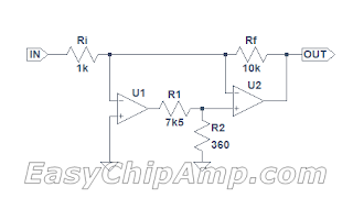
One of the issues with Yewen's topology:

is that R1 R2 (in the schematic above) attenuate the signal amplified by U1, which causes U1 to work extra hard, or, more precisely, work with a higher input signal. As was discussed previously on this blog, this affects the linearity of U1's input stage and adds distortion that cannot be corrected by feedback.

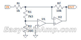
One way to address this issue is to use a better opamp as U1, but it is much easier to move the divider to U1's input:

R1 R2 should be large compared to Ri to avoid an unwanted noise gain increase and a loop gain reduction (see the discussion in my previous post), but otherwise this works exactly the same as Yewen's composite, only with lower distortion.

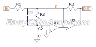
Naturally, this approach also works with frequency dependent dividers:

Friday, January 13, 2023

High Precision Composite Op-Amps, Part 4 - A Practical Composite Chipamp with LM1875

This post is a part of the series on audio amplifier feedback. The contents of the series can be found here.

In my previous post on this topic, I discussed the role of the voltage divider in John D. Yewen's composite op-amps (see his article in Electronics & Wireless World, February 1987) and improving the composite's loop gain at audio frequencies by making the divider frequency dependent.

Towards the end of the previous post, I promised that this approach works in hardware, too, so here are two practical examples.

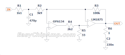
The first is a plain Yewen composite with two dissimilar opamps - an OPA134 and an LM1875:


The divider (R4R5) attenuates the output of the OPA134 by 33/(2200+33)≅-36dB, which together with the opamp's GBW of 8MHz places the zero (see my previous post for an explanation) at about 130kHz. It is kind of low, but in testing, placing the zero at a higher frequency made for poor clipping performance. With such a divider, the OPA134 adds about 16dB of loop gain at 20kHz (more at lower frequencies), and this composite produces 0.003% THD at 1kHz, 20W into 8ohm, or about 1/6 of the distortion of a standalone LM1875.

The second example is a composite with the same opamps and a frequency dependent voltage divider C4C5R10:


The improved divider adds a pole at 2kHz and a zero at 150kHz, increasing the loop gain by another 16dB at 20kHz while maintaining stability and clipping similar to that of the first composite. With a careful PCB layout, this composite should be able to deliver 0.001% of THD at 1kHz, 20W into 8ohm.

Note that for both versions, the Zobel network (R6C2 and R11C6, respectively) with the values shown is required for stability.

Can we make the composite still better? Yes we can! Stay tuned...

Tuesday, September 13, 2022

High Precision Composite Op-Amps, Part 3 - More Loop Gain

This post is a part of the series on audio amplifier feedback. The contents of the series can be found here.

As discussed in my previous post on this topic, the resistive voltage divider in John D. Yewen's composite amplifier (see his article "High-precision composite op-amps" in Electronics & Wireless World, February 1987):

adds a zero to the loop gain, which helps to achieve stability at the expense of the loop gain:

For audio applications, it is desirable to maximize the loop gain, at least in the audio band, but preserve the phase margin. One way to keep that zero and maximize the loop gain at audio frequencies is to make the voltage divider frequency dependent, for example:

Adding an inductor in parallel to R3 adds a pole-zero pair (disregarding the inductor's own series resistance, the pole is at $F_p={1 \over {2 \pi}} {{R_3 || R_4} \over L_1}$, the zero at $F_z={1 \over {2 \pi}} {R_3 \over L_1}$). With the values shown, we get about 12dB of extra loop gain at 20kHz with the same phase margin as without the inductor:

 A 22mH inductor may not be very practical, but a similar effect can be achieved with a resistive-capacitive divider, for example:

Here, the pole is at $F_p={1 \over {2 \pi R_5 (C_1 + C_2)}}$, the zero at $F_z={1 \over {2 \pi R_5 C_1}}$. With the values shown, the loop gain is about the same as with the inductor above:


Not bad for one additional passive component. It works in hardware, too - I will show a practical example in my next post.


Tuesday, September 6, 2022

High Precision Composite Op-Amps, Part 2 - Divide and Conquer

This post is a part of the series on audio amplifier feedback. The contents of the series can be found here.

My previous post on this topic was on composite opamps from by John D. Yewen's article "High-precision composite op-amps" (Electronics & Wireless World, February 1987):

Appropriately choosing the voltage divider R1R2 at the output of U1 allows to achieve stability (obtain sufficient gain and phase margins) of the composite at the expense of the loop gain. Here, orange traces are the loop gain of the composite from the schematic above, while blue are the maximum possible (whether stable or not) loop gain with the same two opamps:

How can a simple resistive divider make the composite stable? Let me look at the role of the voltage divider in Yewen's composite.

Referring to the schematic above, U2 sees a (differential) input signal that is a sum of (i) the signal at the non-inverting output, where Ri and Rf connect, and (ii) the same signal amplifier by U1 and divided by R1R2.

At low frequencies, U1's gain is large, and U2's input signal is effectively that at its non-inverting input. The loop gain is the product of that of U1 and U2 and falls with frequency at 40dB/decade. At high frequencies, U1's gain is small, and U2's input signal is effectively that at its inverting input. The loop gain is just that of U2, falling at 20dB/decade.

The transition from "low" to "high" frequencies is a zero in the composite's loop gain, located at the frequency where the signal magnitudes at the non-inverting and inverting inputs of U2 are equal - that is, when the gain of U2 followed by R1R2 is unity. For a single-pole U1, that frequency is a fraction of U1's Gain Bandwidth Product (GBW):$$F_{zero}=GBW_{U_1} \times {R_2 \over {R_1+R_2}}$$In the example above, GBW is 10MHz, the divider's attenuation is 22, so the zero is at ${{10 MHz}\over 22} = {455 kHz}$.

That is, Yewen's voltage divider sets the frequency of a zero in the composite's loop gain. The higher the attenuation in the divider, the lower is the zero, and vice versa.

By the way, it is possible and quite practical to replace the fixed divider with a trimpot and adjust the zero to one's liking, e.g. to obtain the necessary phase margin.

Can we make it still better? Yes we can! Stay tuned...